★★★Flash Memory: NAND, EEPROM, NVRAM and others [ZT]
another good post:
Everything You Ever Wanted To Know About Semiconductors
Flash Memory Device List
The non-volatile memories are the essential components of the electronics devices. The industry expects a perfect non-volatile memory to meet all requirements for both code and data. However, there is not such perfect memory at all. Alternatively, we have many choices of the flash memories with various parameters including interfaces (data/address buses, protocols and timing), capability (memory density and cost) and reliability (writing endurance and bad blocks). As a result, the designers have to study the available products very carefully to select the suitable components for the projects. In most cases, the system designers have to deploy certain system software components for the specific platforms as well. The software part is so complex that I will cover it in a separate title. Competitive Non-volatile Memories The standard PC architecture adopts a hierarchy structure of memories. The mask ROM and OTP EPROM are used for BIOS. The code and data are stored in the secondary memory devices like the floppy and the hard disk drivers. The code is loaded from the secondary memory devices to DRAM and executes there. A fraction of the loaded code is placed in the high speed cache (SRAM) to improve the system performance. Along with fast development of the silicon storage technologies, the flash memories are widely used in the PC architecture as well. The MTP NOR flash and SPI serial flash memories replace the legacy memories in BIOS. The flash cards and the flash SSD drivers are used as the secondary memory devices in the stylish UMPC and Netbook.
In comparison, the embedded products adopt a wider range of memory types since the embedded hardware platforms are very diverse and tailor-made. Similarly, the flash memories are replacing the legacy non-volatile memories as well. Let us have an overview for the non-volatile memories first. UV-EPROM The UV light erasable EPROM was very popular and widely used as the major code storage media. It is not convenient to reprogram during the development cycle. And its ceramic package is so expensive that the semiconductors manufacturers have to give up and replace it with plastic. EPROM It is commonly named as OTP (One Time Programming) EPROM. It contains the identical UV-EPROM dice in the plastic package. Theoretically, you can erase the chip with the high density energy (UV light) and reprogram it. The engineers can remove the plastic package by acid, erase the read protection bit by UV light and access the binary code (for reverse engineering). However, the advanced processes of the latest chips make them very difficult to erase. EEPROM The Electronics Erasable PROM is a popular non-volatile memory technology to store small mounts of data. The EEPROM is a byte-programmable device as SRAM. The EEPROM has many types with different interfaces, including parallel interface, SPI, I2C and 1-wire. The erasing and programming states are under control of the internal logic and require a charge pump. The EEPROM is usually used to keep the system variables or calibration parameters. The embedded EEPROM can be found in the microcontrollers, RFID and smart cards. Some flash microcontrollers use internal flash block to replace external EEPROM. It is technically achievable but it is not always a good idea since the writing endurance of flash is far less than EEPROM. FeRAM The FeRAM has many advantages over the EEPROM. It runs faster and requires less power. However, it can not dominate the market since EEPROM is very cheap. A few manufacturers (like NEC) use FeRAM in RFID, which can benefit from its fast accessing speed. NVRAM NVRAM is a general term for all non-volatile memories, but hereafter the NVRAM refers to the battery powered SRAM (or DRAM). Dallas/Maxim and ST have shipped many NVRAM products in the microcontroller, RTC and some special ICs. Basic Flash Memories NOR and NAND flash memories are the basic types. They are named according to the internal access interfaces. They are different in the data/address bus, internal block management method, programming speed and writing endurance. In general, the NOR flash is a replacement for the legacy ROM/EPROM for code storage, while the NAND flash is a replacement for the traditional mass storage devices.
NOR (CFI) The NOR flash offers the similar access interface of a RAM. It can be read and programmed on byte or word, but it must be erased by block (or by chip) before programming. Its programming time is also longer than the NAND flash. It can offer so-called XIP (eXecutive In Place) capability for the microprocessors, while NAND flash can not. Although NOR flash is much slower than the memory bus of the modern microprocessors it connects to, it is still acceptable during the initialization period of the whole system. It is widely used in BIOS/bootloader, because the regular microprocessors can not boot from NAND.
The NOR flash has an industrial standard called Common Flash Interface (CFI), which defines a low level command set (chip id, block/unblock, erase chip, erase block and etc.) for the NOR flash. Do not confuse CFI with Compact Flash (CF), which is a memory card standard with IDE and PCMCIA modes.
The traditional NOR flash usually guarantees million of writing endurance cycle to secure the code. However, in many applications, the code or data only requires several times of upgrading. As a result, you can find so-called MTP (Many Times Programming) flash devices available in the market. These chips are very cheap and down-graded for thousands of endurance cycle.
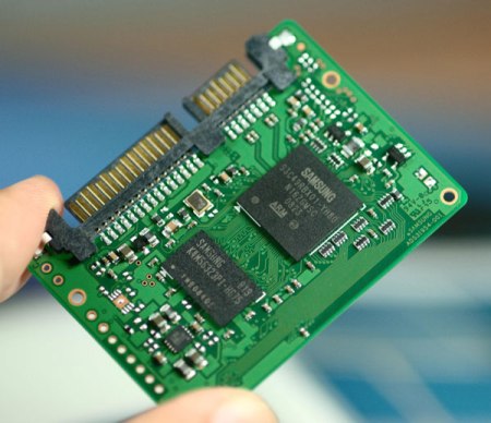
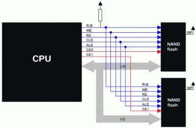
The regular data bus of NOR flash is 8-bit or 16-bit. Exceptionally, NXP puts a 128-bit NOR flash memory in the LPC2000 microcontrollers to speed up the internal memory bus. NAND The NAND flash memory is most commonly used in the secondary memory devices, either in the raw chip (SMC) or managed devices (SD card). Its programming speed is much faster, with larger but less reliable memory blocks. It offers block fashion operations, including read, write, erase, lock and unlock of the specific blocks. The external access bus is identical for different capacities. It can not interface to traditional data/address buses directly, so the code and the data have to be loaded to the RAM first. Additionally, because NAND is not designed as a high reliable memory and its memory block writing endurance cycle is limited, it offers error code correction (ECC) to secure the data integrity. Meanwhile, the memory sub-system has to deploy the bad block management and wear leveling algorithms in the firmware and NAND controller. Besides traditional SLC (Single Level Cell), the MLC can offer multiple levels in single memory cell, which increases the memory density while decreases the writing endurance life cycle.
Although NAND seems to have so many issues (it is not a perfect memory at all), more and more removable memory devices are using NAND flash because the price is so cheap. Also, NAND is the only flash based technology to compete with the hard disk drivers. The popular flash cards are all based upon NAND chips. The SSD product is expanding to the consumer market with the latest Netbook like EeePC. A lot of new players including Intel have released NAND based SATA drivers recently to get the market share from the traditional hard disk driver suppliers. Although the SSD is much expensive than the regular hard disk drivers, I think the SSD can win the competition before long.
Meanwhile, more and more embedded architectures are changing to the cheap NAND flash chips. For example, the previous ARM7TDMI based designs usually use a combination of RAM, NOR and NAND memories. The bootloader usually resides in the NOR to bring up the whole system and initialize the DRAM interface. Then the code in the NAND (like Linux kernel) will be loaded to DRAM or internal SRAM to run. Alternatively, Samsung’s SC2410 ARM920T chip offers NAND boot capability. Its NAND controller can perform the copy operation after reset and load first 4KB code from NAND to the internal RAM and run there. The latest TI OMAP3530 (read the Datasheet 2.0) supports multiple boots from NAND, SD and USB card. The chip has the boot code integrated inside. So the external interface is quite clean and simple. NAND boot is a trend of the boot mode.
Furthermore, all of these memories, RAM, NOR and NAND are going to be merged together by advanced package technology or new variant types. Combo Memories Due the small factor requirement for mobile phones, the new projects look for an all-in-one memory offers all of the interfaces for multiple memories. Some small vendors offered the Combo memories with certain package innovation. The mobile phone manufacturers were fond of these combo devices until they found some new issues. Most of these suppliers are not silicon manufacturers. They bought the dices from different silicon manufacturers and bound them together. Here is a true story: a Combo memory supplier always changes the dices between different suppliers according to the market price. As result, the company gets a lot of complaints from the production lines. Further more, these memories are not always tested!
The silicon suppliers launched new products to meet the requirement of memory convergence. More and more variant flash memories with different combinations are released. Variant Types ORNAND (NOR+NAND) Spansion promotes its ORNAND architecture for the mobile applications. The ORNAND offers low cost NAND memory with high reliability, fast NOR flash. Spansion also offers PoP package for the flash memory, which stacks the flash chip on top of the SoC. The PoP package is quite helpful to reduce the size of PCB with the existing MCP package. However, it reduces the yield as well. OneNAND (RAM+NAND) OneNAND was invented by Samsung, the biggest NAND supplier in the world. OneNAND integrates a small SRAM cache with a NAND memory. This combination offers fast random access, high capacity and low system cost. The code stored in NAND is loaded to the SRAM cache, and then the microprocessor can run the code in the SRAM to implement the XIP. The SRAM size is only 1KB, so it still requires some improvements. Anyway, OneNAND is suitable for the embedded applications. Samsung also offers an embedded bad block management software stack called DataLight OneBoot to offer high reliable data storage management. Based upon OneBoot, the OneBoot+File technology can reduce the system boot up time. This technology works like Hibernate mode in a PC. The state can be restored from previous stored context and thus the system boot is much faster. Serial Flash (SPI) The serial Flash memory is a NOR flash device with SPI interface. The benefit of serial flash memory is reducing the footprint of the IC package and PCB size. With a serial flash, the SoC package cost can be reduced and PCB routing is simplified.
Managed Flash Memories I introduced an open source SD card stack for the LPC213X in one of my blogs (read here: Open source software for FAT file system over MMC SDC). During my research for this topic, I read some inquires about integration SD/MMC cards on board as solid state drivers. Some designers mounted the flash card directly on board without the card slot. However, there are many SD/MMC cards available in BGA package. They are classified as the managed flash memory, which is suitable to be a permanent on-board storage device. All of these devices are under control of disk controllers (SD/MMC/ATA/SATA) and act as disk drivers (hard disk drivers and flash cards). Because the disk controller manages the block management and wear leveling issues, the embedded OS can concentrate on the high level applications.
These devices are not very popular so far. In most cases, the product managers would rather mount a slot on board, instead of purchasing non-standard managed flash memories due to the inventory considerations. Nevertheless, these memories can help us to reduce the PCB size and relieve the memory dependent tasks (wear leveling, block management & etc). All of the managed flash memories have different names (or trade marks) with similar implementations. iNAND (SD) In 2005, SanDisk released iNAND flash memory. It is an embedded storage flash device with a standard SD card controller and MLC NAND flash memory. The biggest iNAND has 4GB NAND flash inside. GBNAND (SD) GBNAND is a trade mark of Toshiba Electronics. This device includes stacked NAND memories, an SD card controller and embedded PSRAM/LP SDRAM. The biggest capacity of GBNAND is 16GB. moviNAND (MMC) Samsung offers moviNAND with the MMC interface. The moviNAND integrates NAND flash memories, an MMC card controller and necessary firmware. e-MMC Micron promotes the e-MMC device to the mobile phone manufacturers. The e-MMC has an MMC card controller and NAND flash memories. The e-MMC is a trade mark of MultiMediaCard Associations. NANDrive (ATA) NANDrive is a trade mark of Silicon Storage Technology, Inc. NANDrive is a solid state drive with NAND flash memories and an ATA controller. It supports PIO mode up to 4 and Multi-word DMA mode up to 2 in a BGA package. mDOC (RAM+Managed NAND) mDOC is a product from MSystems, now part of SanDisk. It is an embedded flash drivers incorporates NAND flash, ATA controller and TrueFFS firmware. SATA SSD There are many SSD products (and CF cards) with ATA interfaces. Now the new designs are switching to the SATA interface. The SSD is quite expensive so far. However the SSD has advantage over the traditional hard disk drivers on anti-shocking, power consumption, data transfer rate and device weight. These benefits make it a perfect choice in a mobile computing device. The latest ATOM based Netbook usually offers two options for the main driver, SSD and HDD. Of course, SSD is a wise choice in a mobile environment. As the fast decline of NAND’s price, more and more consumers will select SSD. Read More Intel Solid-State Drivers and Caching http://www.intel.com/design/flash/nand/index.htm SanDisk mDOC H3
http://www.sandisk.com/OEM/ProductCatalog(1322)-SanDisk_mDOC_H3.aspx
NANDrive from SST http://www.sst.com/products.xhtml/nand_flash_storage/85/ The e-MMC part list of Micron http://www.micron.com/products/nand/managed-nand/partlist What is moviNAND? http://www.samsung.com/global/business/semiconductor/products/fusionmemo… Toshiba’s new MCP integrates Gigabyte NAND flash memory and SD Controller http://www.semicon.toshiba.co.jp/eng/product/memory/selection/topics/117… SanDisk iNAND http://www.sandisk.com/OEM/Default.aspx?CatID=1329 OneNAND from Samsung http://www.samsung.com/global/business/semiconductor/products/fusionmemo… ORNAND from Spansion http://www.spansion.com/flash_memory_products/ORNAND_products.html
转载请注明:在路上 » ★★★Flash Memory: NAND, EEPROM, NVRAM and others [ZT]